Just before 1990, we are explained held condensed matter physics study center. In 1990, facility launched Xiamen Powerway Innovative Material Co., Limited (PAM-XIAMEN), now it is usually a leading manufacturer involving compound semiconductor material inside China.
PAM-XIAMEN develops superior crystal growth and epitaxy technologies, range from typically the first technology Germanium wafer, second systems Gallium Arsenide with essence growth in addition to epitaxy in III-V si doped n-type semiconductor supplies based on Georgia, Ing, In, As as well as L grown by MBE or maybe MOCVD, to the 3 rd generation: Silicon carbide and also Gallium Nitride for DIRECTED and power device program.
Quality is our 1st priority. PAM-XIAMEN has recently been ISO9001: 2008 certified along with given honors from The far east General Supervision of Top quality Supervision, Assessment and Yard. We have possesses in addition to shares four modern day industries, which can provide a significant range of qualified goods to fulfill different needs connected with our consumers.
Welcome an individual to send query, question, inquiry, interrogation to help our sales team when you have further query. Thank you!
Our Background
2011
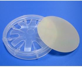
Commercial CdZnTe (CZT) wafer are on size generation, which is any new semiconductor, which usually permits to convert radiation in order to electron effectively, it is definitely mainly utilized in infrared thin-film epitaxy substrate, X-ray as well as γ-ray detection, laser dvd modulation, high-performance solar cellular material and other excellent job areas.
2009
PAM-XIAMEN has transformed often the manufacturing technology to get GaN epitaxy on Blue and also freestanding GaN individual very wafer substrate which can be with regard to UHB-LED and LD. Cultivated by hydride fumes period epitaxy (HVPE) technological know-how, Each of our GaN wafer provides reduced defect density and fewer as well as free macro deficiency denseness.
2007
PAM-XIAMEN grows along with manufactures compound semiconductor substrates-gallium arsenide crystal in addition to wafer. We has used innovative crystal growth technology, straight gradient freeze (VGF) as well as GaAs wafer processing technologies, established a production range from crystal growth, slicing, grinding to polishing digesting and built a 100-class clean room for wafer cleaning and packaging. All of our GaAs wafer include 2~6 inch ingot/wafers for ENCOURAGED, LD and Microelectronics software. Thanks to its excellence associated with molecular beam epitaxy technological innovation (MBE) and Steel Organic and natural Chemical Vapor Deposition(MOCVD), the business can offer planet class epitaxial ingredient semiconductor wafers for microwaves and also RF applications.
04
PAM-XIAMEN has developed SiC crystal clear growth technology and Pareil wafer processing technology, recognized a production line to be able to manufacturer SiC substrate regarding polytype 4H and 6H in different quality marks regarding researcher and market suppliers, Which is utilized in GaN epitaxy product, power equipment, high-temperature system and optoelectronic Devices. Since a professional business put in by the leading makers from the fields involving sophisticated and high-tech substance exploration and state acadamies along with China’s Semiconductor Labrador, we could devoted to continually improve the top quality connected with currently substates in addition to build large size substrates, and also epitaxial technology.
2001
PAM-XIAMEN has established production brand of semiconductor materials rapid Ge(Germanium) Individual Crystals as well as Wafers.
1990
Xiamen Powerway Advanced Substance Co., Ltd(PAM-XIAMEN) founded. PAM-XIAMEN develops enhanced crystal progress and epitaxy technologies, producing processes, manufactured substrates and also semiconductor units.
1990 instructions
We are usually stated owned abridged make a difference physics research heart